


Custom PCB Design & Development
We translate product requirements into a complete PCB design and the files a fabricator needs. Our firmware specialists review every schematic before it goes out, so pin assignments and power states are settled early.
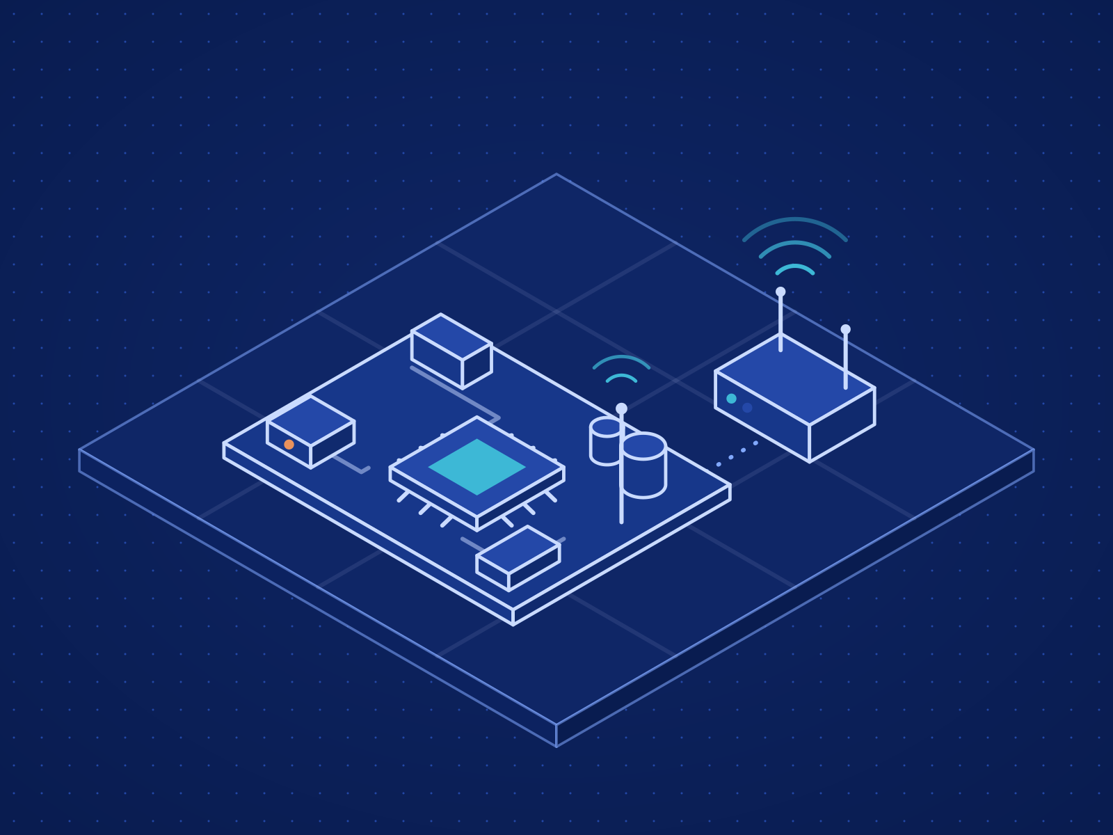
- Network & Connectivity
- Security & Surveillance
- Connected Healthcare
- Smart Cities & Infrastructure
- Fleet & Logistics
- Energy & Smart Utilities
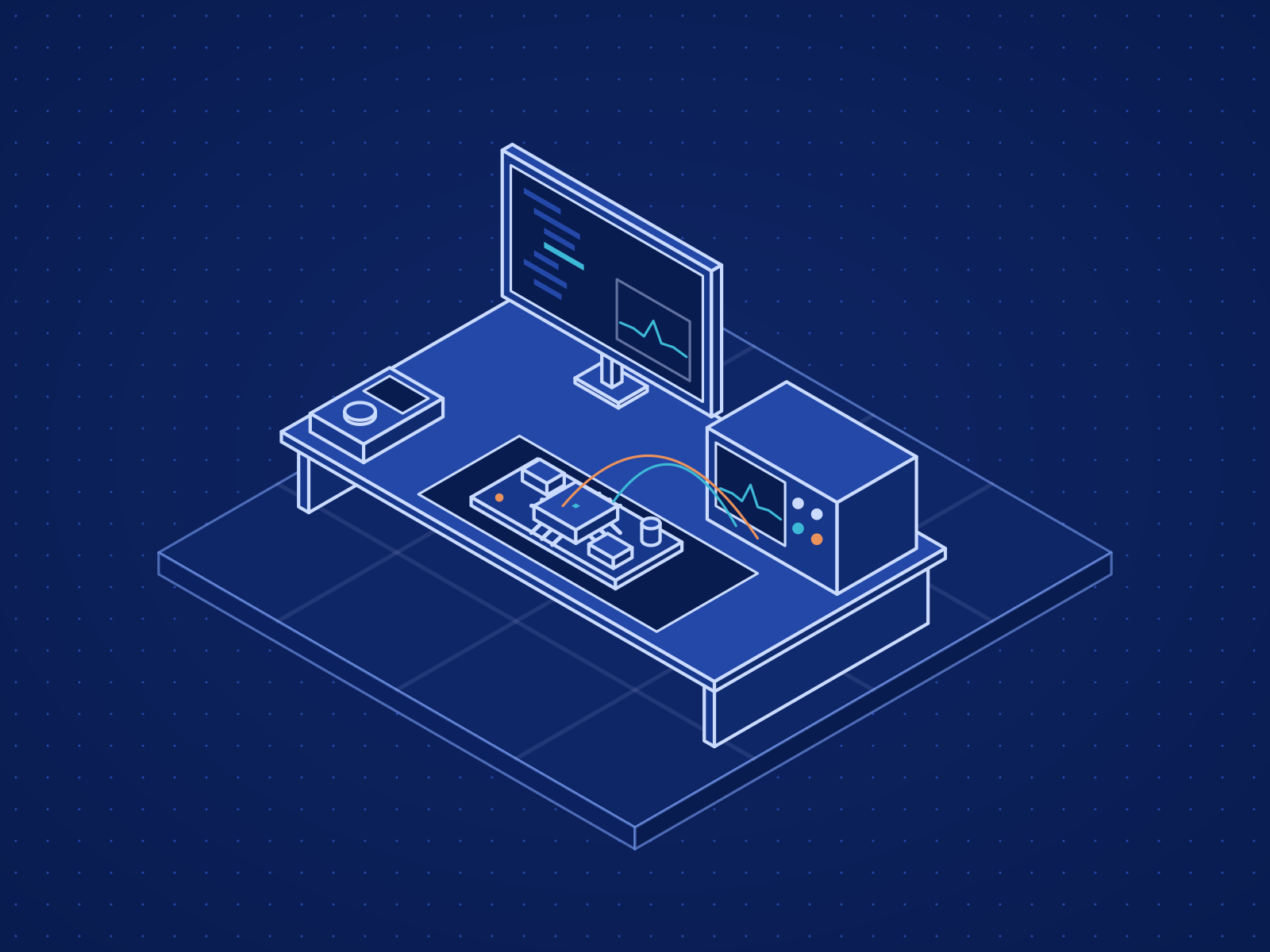
Every Layout Decision Made With Firmware in View
A PCB design is a chain of decisions: which processor, which radios, how the board is powered and what fits inside the enclosure. We make each one with your product and its firmware in view. You receive a schematic, a layout, a bill of materials and fabrication files, all reviewed against your requirements. Fabrication and assembly go to a PCB manufacturer, yours or one of our partners, and when the first boards return we bring them up and test them.
Hardware Capabilities
A requirement becomes a validated prototype, with the firmware and the cloud link designed alongside the board rather than after it.
Schematic Design
Circuits for the processor, power, sensors, radios and interfaces, with the reasoning behind each design choice recorded for your team.
Component Selection
Parts chosen on function, cost, power draw and supply availability, with alternates identified for any part at risk.
PCB Layout
A layout that fits your mechanical constraints, with power, signal and antenna routing treated as design priorities.
Fabrication Package
Fabrication files, bill of materials and assembly drawings, ready for your PCB manufacturer or one of our partners.
Board Bring-Up
First boards powered, checked and tested against real firmware, with every finding carried into the next revision.
Technologies & Delivery Models
Hardware Electronics
The tools we rely on for this layer of the system.
Why KoderTroop for Custom PCB Design & Development
Devices, cloud and applications delivered by one partner, with every decision documented and handed over.
Integrated Hardware and Software Design
Board, firmware and cloud platform share one architecture, so interface decisions are made once and honored at every layer.
Designed for the Field
Power, temperature, enclosure and connectivity at the installation site shape the design from the first schematic.
Prototype to Production-Ready Boards
We design, prototype and validate every board and deliver production-ready files, then support our manufacturing partners through fabrication, assembly and first builds.
You Own the Design Files
Schematics, layout, bill of materials and firmware source are documented and handed to your team at the end of the engagement.

Related Case Studies

Frequently Asked Questions
Your Custom PCB Design & Development Project
Tell us what you are building and the constraints around it. We will scope the work with you.
Requirements & Hardware Architecture
We agree functions, interfaces, power, enclosure and cost targets, then select the processor, radios and principal components.
Circuit Design
We design and review the schematic, with our firmware developers checking pin assignments, peripherals and power states before layout.
PCB Development
We lay out the board to your mechanical constraints and prepare the fabrication and assembly files.
Prototype & Bring-Up
A manufacturing partner fabricates and assembles the prototypes. We power them up, verify each circuit and log every issue.
Firmware Integration & Testing
Firmware runs on the real board and is tested for function, communication, power use and behavior when power or the network drops.
Production Handover & Deployment
We hand over the production package and support pilot builds, field installation and the first devices in service.